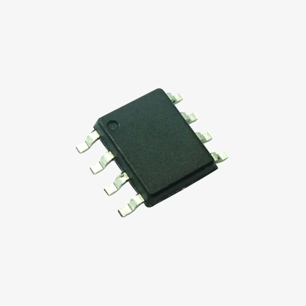
CJQ4459 MOSFET 30V 6.5A SOP-8 SMD Package
The CJQ4459 is an N-channel MOSFET (Metal-Oxide-Semiconductor Field-Effect Transistor) designed for high-efficiency switching and amplification applications. It is housed in an SOP-8 surface-mount device (SMD) package, making it suitable for high-density circuit board layouts. Here’s a detailed description of the product:
Key Features:
- Type: N-Channel MOSFET
- Package: SOP-8 (Small Outline Package)
- Polarity: N-Channel
- Maximum Drain-Source Voltage (Vds): 30V
- Maximum Continuous Drain Current (Id): 6.5A
- Maximum Power Dissipation (Pd): 1.5W
- Low On-Resistance (Rds(on)): Typically 18mΩ at Vgs = 10V
- Gate Threshold Voltage (Vgs(th)): 1V to 3V
Applications:
- Load Switching: Ideal for switching low-voltage loads.
- Power Management: Suitable for use in power management applications in portable devices.
- Battery-Powered Applications: Commonly used in battery-powered applications due to its low on-resistance and high efficiency.
- DC-DC Converters: Can be used in DC-DC converter circuits for efficient power conversion.
Pin Configuration:
- Pin 1 (G): Gate
- Pin 2 (S): Source
- Pin 3 (S): Source
- Pin 4 (S): Source
- Pin 5 (D): Drain
- Pin 6 (D): Drain
- Pin 7 (D): Drain
- Pin 8 (D): Drain
Electrical Characteristics:
- Drain-Source Voltage (Vds): 30V max
- Gate-Source Voltage (Vgs): ±20V max
- Continuous Drain Current (Id): 6.5A max
- Power Dissipation (Pd): 1.5W max
- On-Resistance (Rds(on)): 18mΩ typical at Vgs = 10V
- Total Gate Charge (Qg): 9nC typical
- Turn-On Delay Time (td(on)): 10ns typical
- Turn-Off Delay Time (td(off)): 25ns typical
Note: Product images are for illustrative purposes only and may differ from the actual product.
Original: $0.16
-63%$0.16
$0.06Description
The CJQ4459 is an N-channel MOSFET (Metal-Oxide-Semiconductor Field-Effect Transistor) designed for high-efficiency switching and amplification applications. It is housed in an SOP-8 surface-mount device (SMD) package, making it suitable for high-density circuit board layouts. Here’s a detailed description of the product:
Key Features:
- Type: N-Channel MOSFET
- Package: SOP-8 (Small Outline Package)
- Polarity: N-Channel
- Maximum Drain-Source Voltage (Vds): 30V
- Maximum Continuous Drain Current (Id): 6.5A
- Maximum Power Dissipation (Pd): 1.5W
- Low On-Resistance (Rds(on)): Typically 18mΩ at Vgs = 10V
- Gate Threshold Voltage (Vgs(th)): 1V to 3V
Applications:
- Load Switching: Ideal for switching low-voltage loads.
- Power Management: Suitable for use in power management applications in portable devices.
- Battery-Powered Applications: Commonly used in battery-powered applications due to its low on-resistance and high efficiency.
- DC-DC Converters: Can be used in DC-DC converter circuits for efficient power conversion.
Pin Configuration:
- Pin 1 (G): Gate
- Pin 2 (S): Source
- Pin 3 (S): Source
- Pin 4 (S): Source
- Pin 5 (D): Drain
- Pin 6 (D): Drain
- Pin 7 (D): Drain
- Pin 8 (D): Drain
Electrical Characteristics:
- Drain-Source Voltage (Vds): 30V max
- Gate-Source Voltage (Vgs): ±20V max
- Continuous Drain Current (Id): 6.5A max
- Power Dissipation (Pd): 1.5W max
- On-Resistance (Rds(on)): 18mΩ typical at Vgs = 10V
- Total Gate Charge (Qg): 9nC typical
- Turn-On Delay Time (td(on)): 10ns typical
- Turn-Off Delay Time (td(off)): 25ns typical
Note: Product images are for illustrative purposes only and may differ from the actual product.