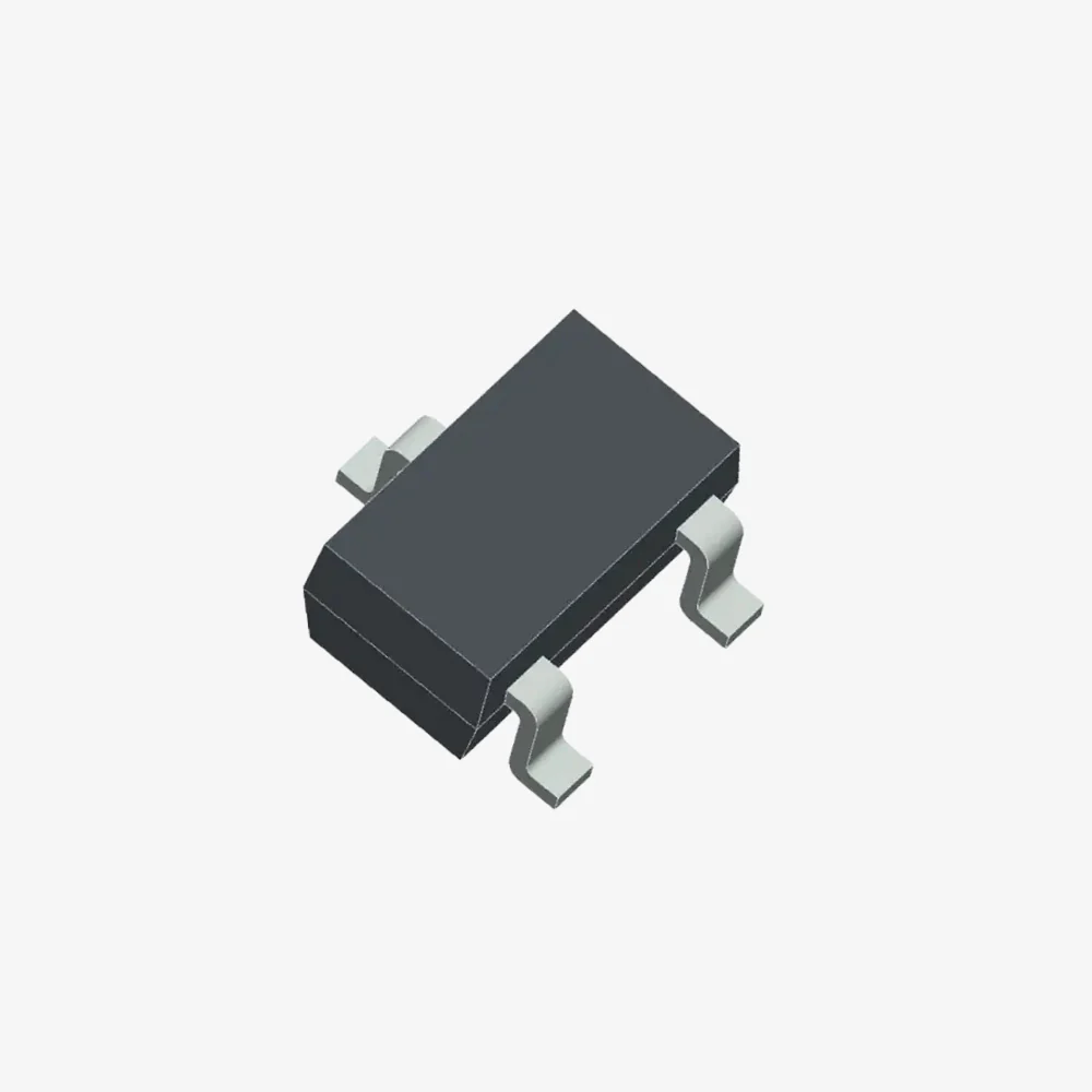
MMUN2233LT1G Transistor SOT-23 SMD Package
The MMUN2233LT1G is a unique NPN transistor integrated with a monolithic bias resistor network, simplifying circuit design and reducing component count. It is housed in a compact SOT-23 surface-mount device (SMD) package, suitable for high-density circuit board layouts. Here is a detailed description of the product:
Key Features:
-
Type: NPN Bipolar Junction Transistor with Monolithic Bias Resistor Network
-
Package: SOT-23 (Surface Mount Device)
-
Polarity: NPN
-
Maximum Collector-Emitter Voltage (Vceo): 50V
-
Maximum Collector Current (Ic): 10mA
-
Monolithic Bias Resistor Network: Integrated resistors for easy biasing
-
Maximum Power Dissipation (Pd): 350mW
-
Operating Temperature Range: -55°C to +150°C
Applications:
-
Switching Applications: Ideal for low-current switching applications.
-
Signal Conditioning: Suitable for signal conditioning and interface applications.
-
Digital Circuits: Commonly used in digital circuits requiring transistor logic level shifts and signal amplification.
Physical Dimensions:
-
Length: Approximately 2.92mm
-
Width: Approximately 1.3mm
-
Height: Approximately 1.1mm
Pin Configuration:
-
Pin 1 (Emitter): This is the emitter terminal, which is typically grounded in common-emitter configurations.
-
Pin 2 (Base): The base terminal, used to control the transistor's switching and amplification.
-
Pin 3 (Collector): The collector terminal, through which the main current flows when the transistor is in the 'on' state.
Note: Product images are for illustrative purposes only and may differ from the actual product.
Description
The MMUN2233LT1G is a unique NPN transistor integrated with a monolithic bias resistor network, simplifying circuit design and reducing component count. It is housed in a compact SOT-23 surface-mount device (SMD) package, suitable for high-density circuit board layouts. Here is a detailed description of the product:
Key Features:
-
Type: NPN Bipolar Junction Transistor with Monolithic Bias Resistor Network
-
Package: SOT-23 (Surface Mount Device)
-
Polarity: NPN
-
Maximum Collector-Emitter Voltage (Vceo): 50V
-
Maximum Collector Current (Ic): 10mA
-
Monolithic Bias Resistor Network: Integrated resistors for easy biasing
-
Maximum Power Dissipation (Pd): 350mW
-
Operating Temperature Range: -55°C to +150°C
Applications:
-
Switching Applications: Ideal for low-current switching applications.
-
Signal Conditioning: Suitable for signal conditioning and interface applications.
-
Digital Circuits: Commonly used in digital circuits requiring transistor logic level shifts and signal amplification.
Physical Dimensions:
-
Length: Approximately 2.92mm
-
Width: Approximately 1.3mm
-
Height: Approximately 1.1mm
Pin Configuration:
-
Pin 1 (Emitter): This is the emitter terminal, which is typically grounded in common-emitter configurations.
-
Pin 2 (Base): The base terminal, used to control the transistor's switching and amplification.
-
Pin 3 (Collector): The collector terminal, through which the main current flows when the transistor is in the 'on' state.
Note: Product images are for illustrative purposes only and may differ from the actual product.